Let
us now look at
combinational circuits. Then we will move
on to sequential circuits. If you wish
to skip immediately to sequential circuits,
use the navigational links at the top
of this page to select the type of circuit
you would like to examine.
-
XOR Function -
On
the previous page we stated that the Exclusive-OR,
or XOR function can be described verbally
as, "Either A or B, but not both."
In the realm of digital logic there are
several ways of stating this in a more
detailed and precise format. We won't
go here into such devices as Truth tables
and graphic representations. We will stick
with the more complete verbal statement,
"NOT A and B, or A and NOT B."
The
circuit required to implement this description
is shown below:
There
are many ways in which the simple logic
gates we have examined can be combined
to perform useful functions. Some of these
circuits produce outputs which are only
dependent upon the current logic states
of all inputs. These are called combinational
logic circuits. Other circuits are designed
to actually remember the past states of
their inputs, and to produce outputs based
on those past signals as well as the current
states of their inputs. These circuits
can act in accordance with a sequence
of input signals, and are therefore known
as sequential logic circuits.
A
key requirement of digital computers is
the ability to use logical functions to
perform arithmetic operations. The basis
of this is addition; if we can add two
binary numbers, we can just as easily
subtract them, or get a little fancier
and perform multiplication and division.
How, then, do we add two binary numbers?
Let's start by adding two binary bits.
Since each bit has only two possible values,
0 or 1, there are only four possible combinations
of inputs. These four possibilities, and
the resulting sums, are:
0
+
0
=
0
0
+
1
=
1
1
+
0
=
1
1
+
1
=
10
Fourth line indicates that we have to
account for two output bits when we add
two input bits: the sum and a possible
carry. Let's set this up as a truth table
with two inputs and two outputs, and see
where we can go from there.
The Carry output is a simple AND function,
and the Sum is an Exclusive-OR. Thus,
we can use two gates to add these two
bits together. The resulting circuit is
shown below:
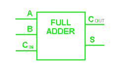
To construct a full adder circuit, we'll
need three inputs and two outputs. Since
we'll have both an input carry and an
output carry, we'll designate them as
CIN and COUT. At the same time, we'll
use S to designate the final Sum output.
Here is the resulting truth table:
INPUTS
OUTPUTS
A
B
CIN
COUT
S
0
0
0
0
0
0
0
1
0
1
0
1
0
0
1
0
1
1
1
0
1
0
0
0
1
1
0
1
1
0
1
1
0
1
0
1
1
1
1
1
It looks as if COUT may be either an AND
or an OR function, depending on the value
of A, and S is either an XOR or an XNOR,
again depending on the value of A. Looking
a little more closely, however, we can
note that the S output is actually an
XOR between the A input and the half-adder
SUM output with B and CIN inputs. Also,
the output carry will be true if any two
or all three inputs are logic 1.
What this suggests is also intuitively
logical: we can use two half-adder circuits.
The first will add A and B to produce
a partial Sum, while the second will add
CIN to that Sum to produce the final S
output. If either half-adder produces
a carry, there will be an output carry.
Thus, COUT will be an OR function of the
half-adder Carry outputs. The resulting
full adder circuit is shown below:
The circuit above is really too complicated
to be used in larger logic diagrams, so
a separate symbol, shown at the bottom,
is used to represent a one-bit full adder.
In fact, it is common practice in logic
diagrams to represent any complex function
as a "black box" with input
and output signals designated. It is,
after all, the logical function that is
important, not the exact method of performing
that function.
This is a digital circuit with multiple
signal inputs, one of which is selected
by separate address inputs to be sent
to the single output. It's not easy to
describe without the logic diagram, but
is easy to understand when the diagram
is available.
A two-input multiplexer is shown below:
The
multiplexer circuit is typically used
to combine two or more digital signals
onto a single line, by placing them there
at different times. Technically, this
is known as time-division multiplexing.
Input
A is the addressing input, which controls
which of the two data inputs, X0 or X1,
will be transmitted to the output. If
the A input switches back and forth at
a frequency more than double the frequency
of either digital signal, both signals
will be accurately reproduced, and can
be separated again by a demultiplexer
circuit synchronized to the multiplexer.
This is not as difficult as it may seem
at first glance; the telephone network
combines multiple audio signals onto a
single pair of wires using exactly this
technique, and is readily able to separate
many telephone conversations so that everyone's
voice goes only to the intended recipient.
With the growth of the Internet and the
World Wide Web, most people have heard
about T1 telephone lines. A T1 line can
transmit up to 24 individual telephone
conversations by multiplexing them in
this manner.
The
opposite of the multiplexer circuit, logically
enough, is the demultiplexer. This circuit
takes a single data input and one or more
address inputs, and selects which of multiple
outputs will receive the input signal.
The same circuit can also be used as a
decoder, by using the address inputs as
a binary number and producing an output
signal on the single output that matches
the binary address input. In this application,
the data input line functions as a circuit
enabler — if the circuit is disabled,
no output will show activity regardless
of the binary input number.
A
one-line to two-line decoder/demultiplexer
is shown below:
This
circuit uses the same AND gates and the
same addressing scheme as the two-input
multiplexer circuit shown in these pages.
The basic difference is that it is the
inputs that are combined and the outputs
that are separate. By making this change,
we get a circuit that is the inverse of
the two-input multiplexer. If you were
to construct both circuits on a single
breadboard, connect the multiplexer output
to the data IN of the demultiplexer, and
drive the (A)ddress inputs of both circuits
with the same signal, you would find that
the initial X0 input would be transmitted
to OUT0 and the X1 input would reach only
OUT1.
The one problem with this arrangement
is that one of the two outputs will be
inactive while the other is active. To
retain the output signal, we need to add
a latch circuit that can follow the data
signal while it's active, but will hold
the last signal state while the other
data signal is active. An excellent circuit
for this is the D (or Data) Latch. By
placing a latch after each output and
using the Addressing input (or its inverse)
to control them, we can maintain both
output signals at all times. If the Address
input changes much more rapidly than the
data inputs, the output signals will match
the inputs
faithfully.