In
order for a logical circuit to "remember"
and retain its logical state even after
the controlling input signal(s) have been
removed, it is necessary for the circuit
to include some form of feedback. We might
start with a pair of inverters, each having
its input connected to the other's output.
The two outputs will always have opposite
logic levels.
The
problem with this is that we don't have
any additional inputs that we can use
to change the logic states if we want.
We can solve this problem by replacing
the inverters with NAND or NOR gates,
and using the extra input lines to control
the circuit.
The
circuit shown below is a basic NAND latch.
The inputs are generally designated "S"
and "R" for "Set"
and "Reset" respectively. Because
the NAND inputs must normally be logic
1 to avoid affecting the latching action,
the inputs are considered to be inverted
in this circuit.
The
outputs of any single-bit latch or memory
are traditionally designated Q and Q'.
In a commercial latch circuit, either
or both of these may be available for
use by other circuits. In any case, the
circuit itself is:
For
the NAND latch circuit, both inputs should
normally be at a logic 1 level. Changing
an input to a logic 0 level will force
that output to a logic 1. The same logic
1 will also be applied to the second input
of the other NAND gate, allowing that
output to fall to a logic 0 level. This
in turn feeds back to the second input
of the original gate, forcing its output
to remain at logic 1.
Applying
another logic 0 input to the same gate
will have no further effect on this circuit.
However, applying a logic 0 to the other
gate will cause the same reaction in the
other direction, thus changing the state
of the latch circuit the other way.
Note
that it is forbidden to have both inputs
at a logic 0 level at the same time. That
state will force both outputs to a logic
1, overriding the feedback latching action.
In this condition, whichever input goes
to logic 1 first will lose control, while
the other input (still at logic 0) controls
the resulting state of the latch. If both
inputs go to logic 1 simultaneously, the
result is a "race" condition,
and the final state of the latch cannot
be determined ahead of time.
While
most of our demonstration circuits use
NAND gates, the same functions can also
be performed using NOR gates. A few adjustments
must be made to allow for the difference
in the logic function, but the logic involved
is quite similar.
The
circuit shown below is a basic NOR latch.
The inputs are generally designated "S"
and "R" for "Set"
and "Reset" respectively. Because
the NOR inputs must normally be logic
0 to avoid overriding the latching action,
the inputs are not inverted in this circuit.
The NOR-based latch circuit is:
For
the NOR latch circuit, both inputs should
normally be at a logic 0 level. Changing
an input to a logic 1 level will force
that output to a logic 0. The same logic
0 will also be applied to the second input
of the other NOR gate, allowing that output
to rise to a logic 1 level. This in turn
feeds back to the second input of the
original gate, forcing its output to remain
at logic 0 even after the external input
is removed.
Applying
another logic 1 input to the same gate
will have no further effect on this circuit.
However, applying a logic 1 to the other
gate will cause the same reaction in the
other direction, thus changing the state
of the latch circuit the other way.
Note
that it is forbidden to have both inputs
at a logic 1 level at the same time. That
state will force both outputs to a logic
0, overriding the feedback latching action.
In this condition, whichever input goes
to logic 0 first will lose control, while
the other input (still at logic 1) controls
the resulting state of the latch. If both
inputs go to logic 0 simultaneously, the
result is a "race" condition,
and the final state of the latch cannot
be determined ahead of time.
By
adding a pair of NAND gates to the input
circuits of the RS latch, we accomplish
two goals: normal rather than inverted
inputs, and a third input common to both
gates which we can use to synchronize
this circuit with others of its kind.
The
clocked RS NAND latch is shown below:
The
clocked RS latch circuit is very similar
in operation to the basic latch. The S
and R inputs are normally at logic 0,
and must be changed to logic 1 to change
the state of the latch. However, with
the third input, a new factor has been
added. This input is typically designated
C or CLK, because it is typically controlled
by a clock circuit of some sort, which
is used to synchronize several of these
latch circuits with each other. The output
can only change state while the CLK input
is a logic 1. When CLK is a logic 0, the
S and R inputs will have no effect.
The
same rule about not activating both the
S and R inputs simultaneously holds true:
if both are logic 1 when the clock is
also logic 1, the latching action is bypassed
and both outputs will go to logic 1. The
difference in this case is that if the
CLK input drops to logic 0 first, there
is no question or doubt -- a true race
condition will exist, and you cannot tell
which way the outputs will come to rest.
The example circuit on this page reflects
this uncertainty.
For
correct operation, the selected R or S
input should be brought to logic 1, then
the CLK input should be made logic 1 and
then logic 0 again. Finally, the selected
input should be returned to logic 0.
The
clocked RS latch solves some of the problems
of basic RS latch circuit, and allows
closer control of the latching action.
However, it is by no means a complete
solution. A major problem remaining is
that this latch circuit could easily experience
a change in S and R input levels while
the CLK input is still at a logic 1 level.
This allows the circuit to change state
many times before the CLK input returns
to logic 0.
One
way to minimize this problem is to keep
the CLK at logic 0 most of the time, and
to allow only brief changes to logic 1.
However, this approach still cannot guarantee
that the latch will only change state
once while the clock signal is at logic
1. This signal must have a certain duration
to make sure all latches have time to
respond to it, and in that time, most
latches can respond to multiple changes.
To
adjust the clocked RS latch for edge triggering,
we must actually combine two identical
clocked latch circuits, but have them
operate on opposite halves of the clock
signal. The resulting circuit is commonly
called a flip-flop, because its output
can first flip one way and then flop back
the other way. The clocked RS latch is
also sometimes called a flip-flop, although
it is more properly referred to as a latch
circuit.
The
two-section flip-flop is also known as
a master-slave flip-flop, because the
input latch operates as the master section,
while the output section is slaved to
the master during half of each clock cycle.
The
edge-triggered RS NAND flip-flop is shown
below:
The
edge-triggered RS flip-flop actually consists
of two identical RS latch circuits, as
shown above. However, the inverter connected
between the two CLK inputs ensures that
the two sections will be enabled during
opposite half-cycles of the clock signal.
This is the key to the operation of this
circuit.
If
we start with the CLK input at logic 0
as initially depicted above, the S and
R inputs are disconnected from the input
(master) latch. Therefore, any changes
in the input signals cannot affect the
state of the final outputs.
When
the CLK signal goes to logic 1, the S
and R inputs are able to control the state
of the input latch, just as with the single
RS latch circuit you already examined.
However, at the same time the inverted
CLK signal applied to the output (slave)
latch prevents the state of the input
latch from having any effect here. Therefore,
any changes in the R and S input signals
are tracked by the input latch while CLK
is at logic 1, but are not reflected at
the Q and Q' outputs.
When
CLK falls again to logic 0, the S and
R inputs are again isolated from the input
latch. At the same time, the inverted
CLK signal now allows the current state
of the input latch to reach the output
latch. Therefore, the Q and Q' outputs
can only change state when the CLK signal
falls from a logic 1 to logic 0. This
is known as the falling edge of the CLK
signal; hence the designation edge-triggered
flip-flop.
One
very useful variation on the RS latch
circuit is the Data latch, or D latch
as it is generally called. As shown in
the logic diagram below, the D latch is
constructed by using the inverted S input
as the R input signal. The single remaining
input is designated "D" to distinguish
its operation from other types of latches.
It makes no difference that the R input
signal is effectively clocked twice, since
the CLK signal will either allow the signals
to pass both gates or it will not.
For
comparison, you can review the RS NAND
latch circuit if you wish.
In
the D latch, when the CLK input is logic
1, the Q output will always reflect the
logic level present at the D input, no
matter how that changes. When the CLK
input falls to logic 0, the last state
of the D input is trapped and held in
the latch, for use by whatever other circuits
may need this signal.
Because
the single D input is also inverted to
provide the signal to reset the latch,
this latch circuit cannot experience a
"race" condition caused by all
inputs being at logic 1 simultaneously.
Therefore the D latch circuit can be safely
used in any circuit.
Although
the internal circuitry of latches and
flip-flops is interesting to watch on
an individual basis, placing all of those
logic symbols in a diagram involving multiple
flip-flops would rapidly generate so much
clutter that the overall purpose of the
diagram would be lost. To avoid this problem,
we use the "black-box" approach.
This is actually just one step further
that the "black-box" approach
we used in specifying logic gate symbols
to represent specific clusters of electronic
components — now we are using one
symbol to represent a cluster of logic
gates connected to perform a specific
function.
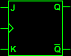
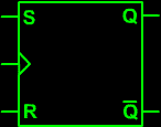
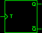
Some
typical flip-flop symbols are shown below:
Any
of these symbols may be modified according
to their actual use within the larger
circuit. For example, if only the Q output
is used, it may well be the only output
shown. Some flip-flops incorporate master
preset or reset inputs, which bypass the
clock and the master section of an edge-triggered
flip-flop and force the output to an immediate
known state. This is often used when a
circuit comprised of many flip-flops is
first powered up, so that all circuits
will start in a known state.